When a Chip Keeps Shutting Down, and the Lab Can't Tell You Why
At a Glance
The Failure Nobody Could Explain
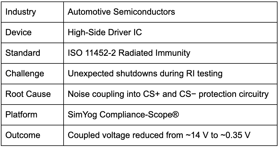
A leading automotive semiconductor company was qualifying an automotive smart High-Side Driver IC designed for applications including power distribution boxes, body control modules and DC/DC converter systems.
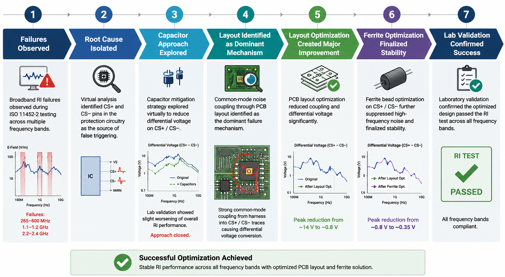
During ISO 11452-2 radiated immunity testing, the device repeatedly shut down when exposed to electromagnetic fields. The failures were not random. They appeared consistently across three frequency ranges: 265–600 MHz, 1.1–1.2 GHz, and 2.2–2.4 GHz. Once the field exposure stopped, the device recovered and resumed normal operation.
The behaviour suggested that one of the device's protection mechanisms was being falsely triggered. But knowing that a protection circuit was tripping was only the beginning. The real question was what was causing it.
The laboratory could identify the failure bands. It could confirm that a shutdown had occurred. What it could not show was how electromagnetic energy was entering the system, where it was coupling, or which part of the design was most susceptible and responsible.
Narrowing Down the Suspects
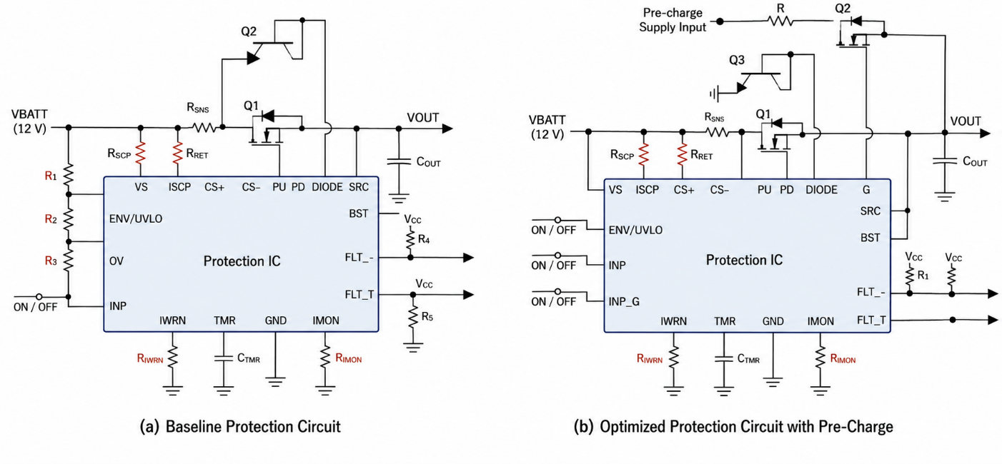
The device included multiple integrated protection mechanisms:
- Overcurrent Protection (OCP)
- Short-Circuit Protection (SCP)
- Overtemperature Protection (OTP)
- Diagnostic Monitoring Circuitry
To isolate the source of the problem, the engineering team performed a series of additional chamber tests, selectively enabling and disabling individual protection functions.The investigation ruled out the overtemperature path. The failures only appeared when the overcurrent and short-circuit protection circuitry remained active.
This significantly narrowed the search area, but it still didn't explain the failure mechanism. The team now knew which subsystem was involved. They still didn't know how electromagnetic energy was reaching it.
Recreating the Entire Test Environment Virtually
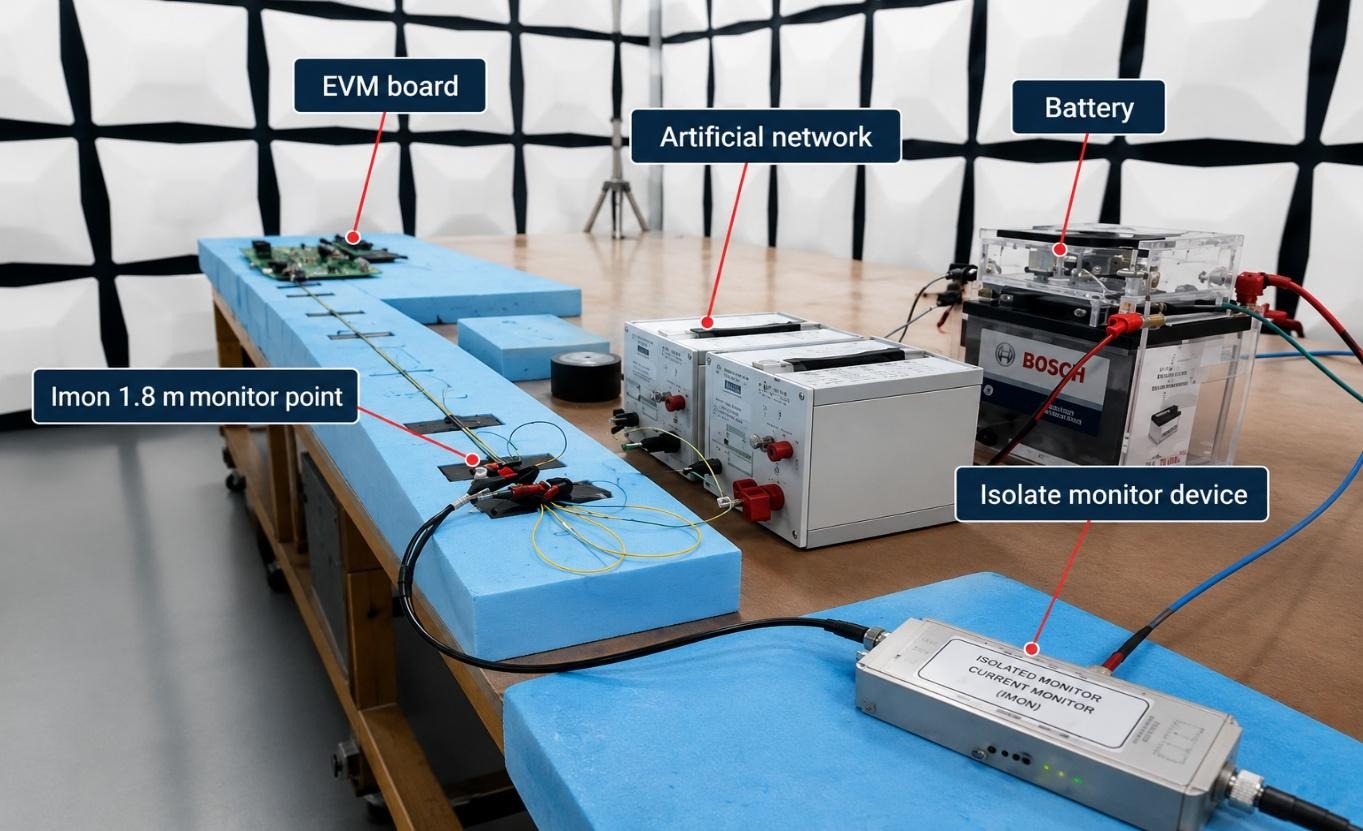
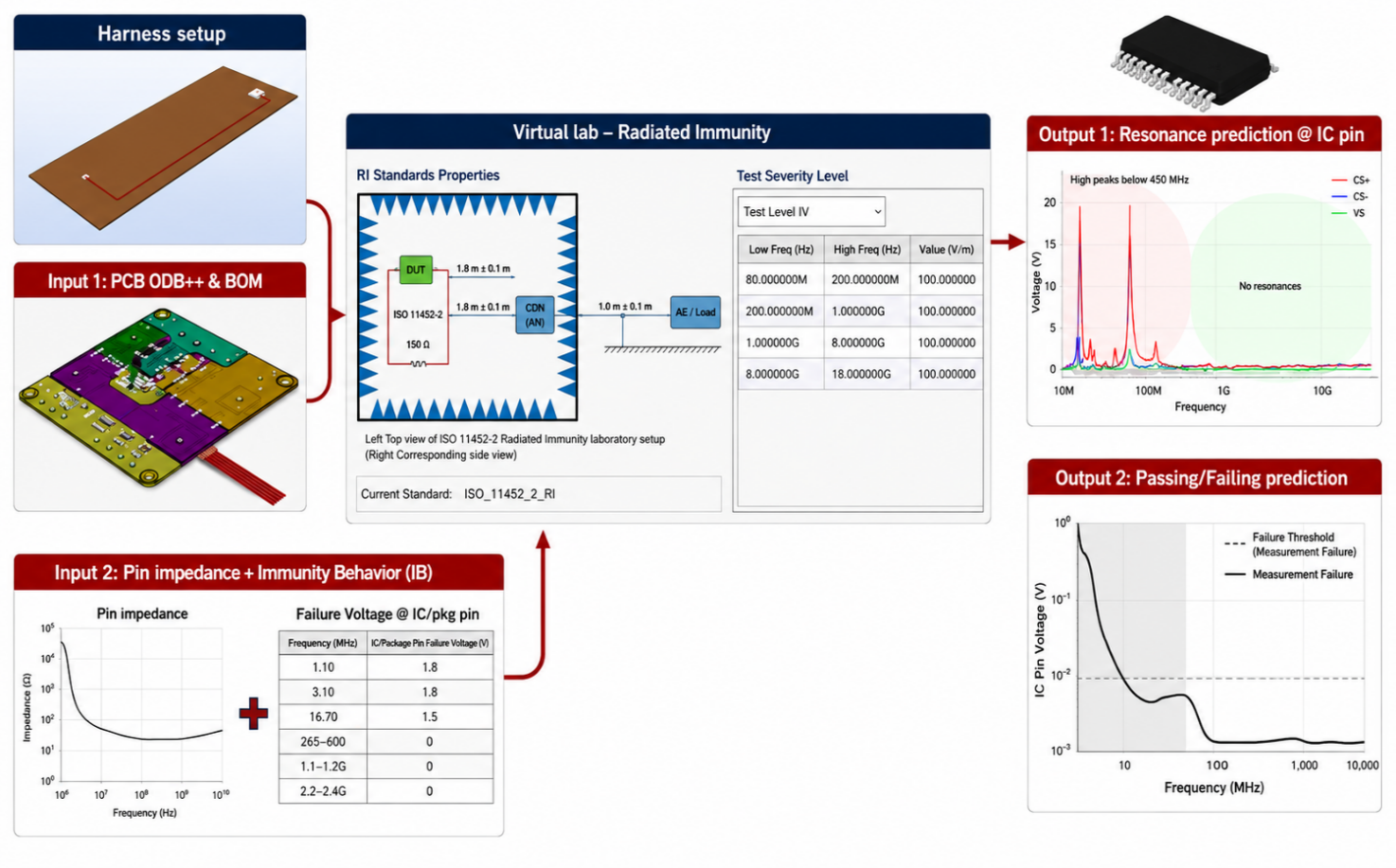
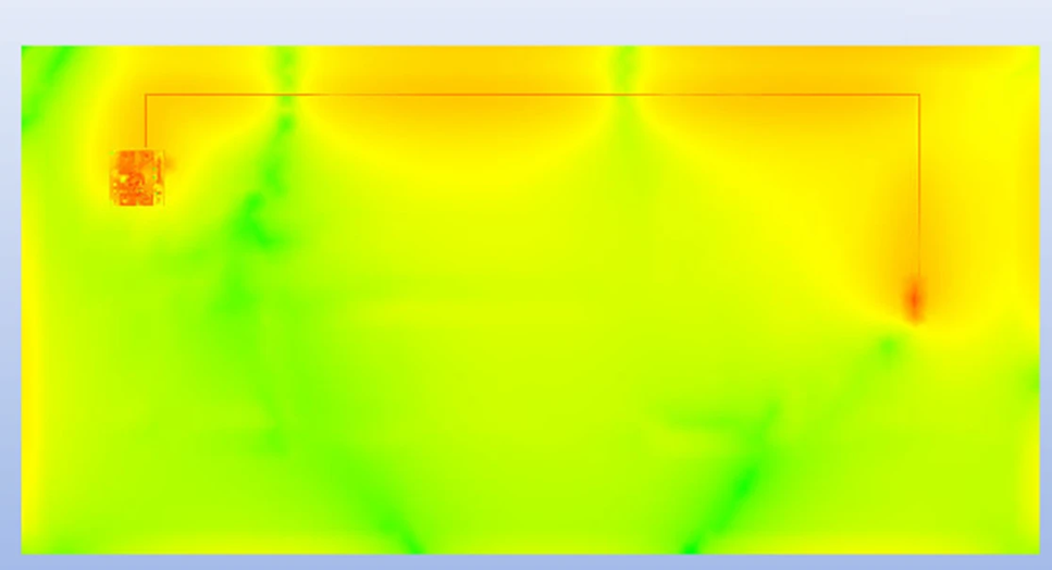
To gain that visibility, the team recreated the complete ISO 11452-2 environment using SimYog's Compliance-Scope® platform.
The virtual model included:
- A replicated ISO 11452-2 RI environment
- The EVM PCB layout and the bill of materials
- The cable harness representation
- Antenna excitation configuration
- Test setup geometry
- Critical IC pins and their electrical behaviour
- Frequency-dependent passive component modeling
- Coupled EM-circuit analysis
The objective was straightforward: reproduce the failure virtually and observe what could not be measured directly in the chamber. By monitoring voltage behaviour at individual IC pins across frequency, the team could investigate the actual susceptibility paths inside the design.
The Breakthrough
Using Compliance-Scope®, engineers evaluated multiple mitigation strategies.The simulation quickly revealed a clear pattern.
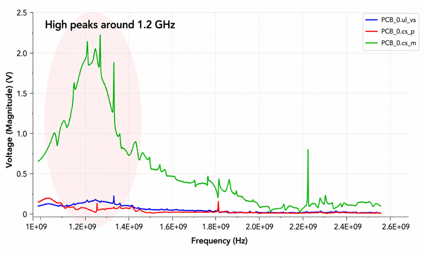
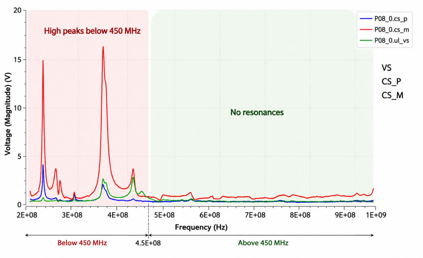
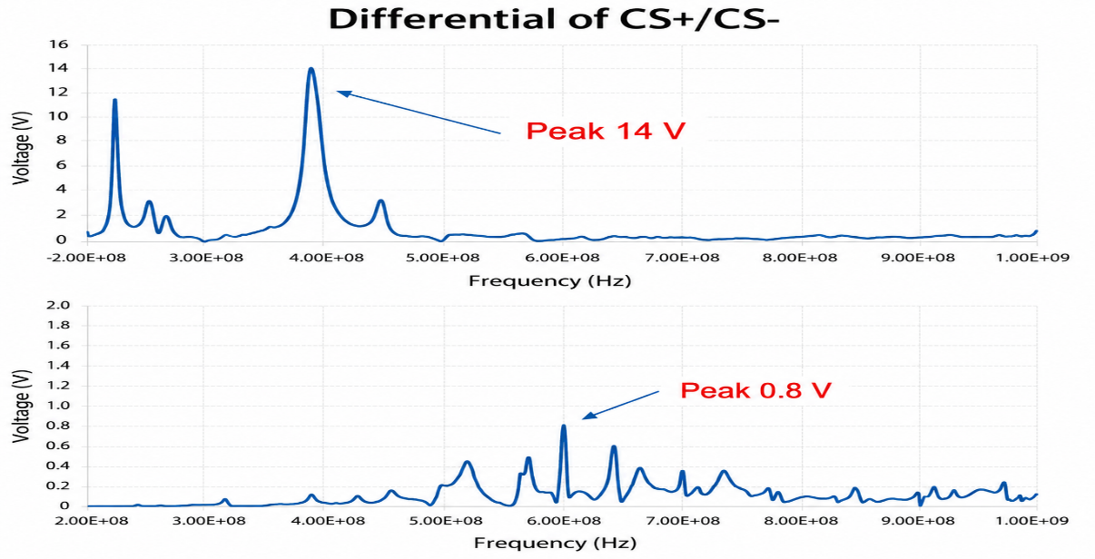
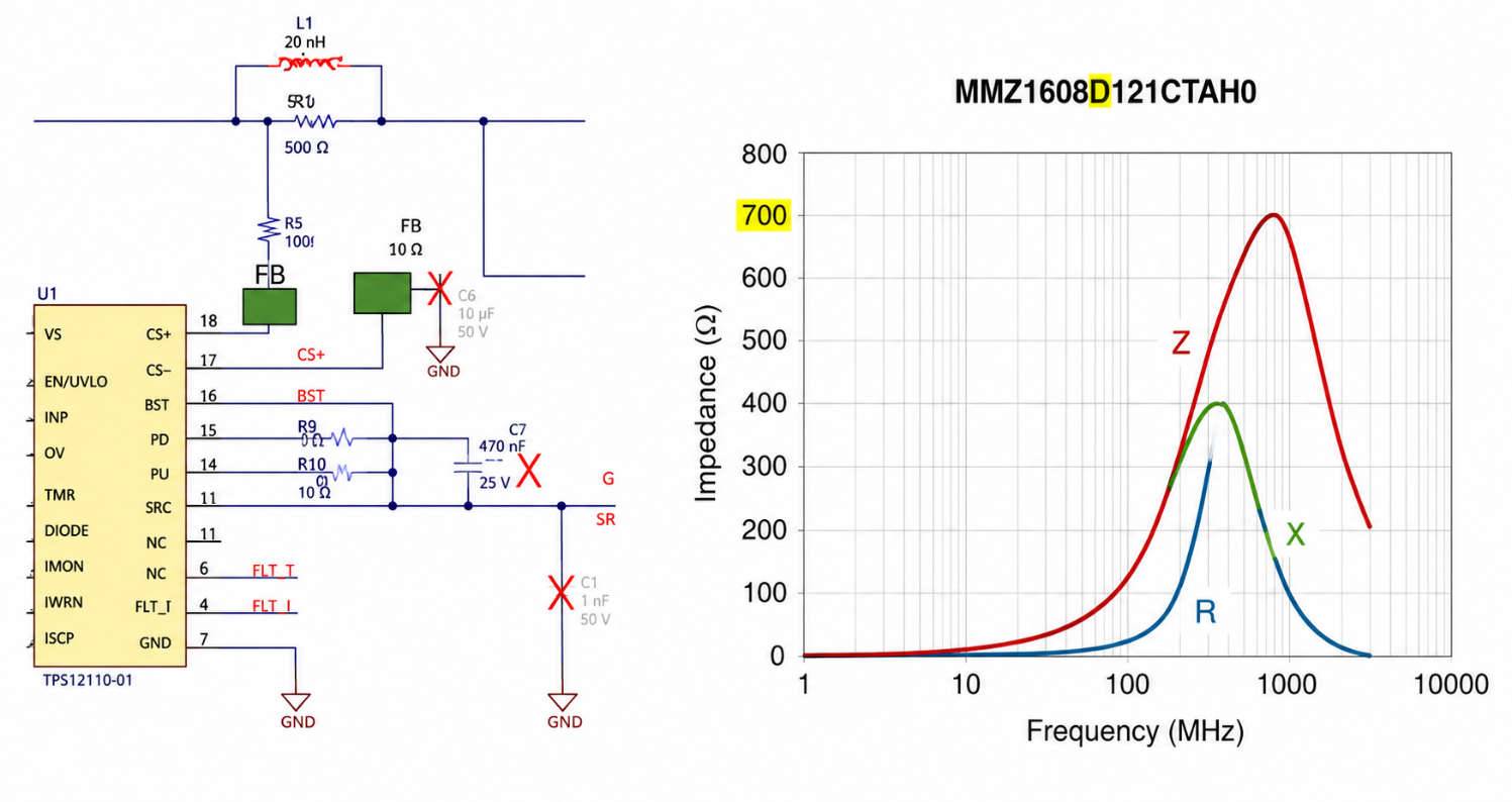
Most monitored signals showed relatively low levels of coupled energy. Two pins stood out immediately: CS+ and CS−, the current-sense inputs connected to the overcurrent and short-circuit protection circuitry.
Across the same frequency regions where failures were observed in the chamber, these pins exhibited pronounced voltage peaks.
In the most severe region, the differential voltage between CS+ and CS− approached 14 V.
The device's protection threshold was approximately 14.5 V.
For the first time, the team could see exactly why the shutdowns were occurring. Electromagnetic energy was being absorbed by the cable harness, transferred onto the PCB, and converted into differential noise at the sensitive protection inputs. Under certain conditions, the induced voltage became large enough to falsely trigger the protection circuitry and shut the device down.
The problem was no longer an unexplained compliance failure. It had a specific mechanism, a specific signal path, and a measurable target for improvement.
Testing Solutions Before Touching Hardware
With the root cause identified, the next step was determining how to reduce susceptibility. Rather than modifying hardware immediately, the team evaluated multiple mitigation strategies inside the virtual environment.
Attempt 1: Add a Capacitor
The first idea was simple: place a capacitor between CS+ and CS− to suppress differential noise. Initially, the approach looked promising. Some improvement was observed at lower frequencies.
However, the simulation also revealed a new problem.
The capacitor interacted with existing PCB parasitics and introduced additional resonances in other frequency regions. When laboratory testing was performed, the results matched the simulation closely. The capacitor-only solution did not improve overall radiated immunity performance and slightly worsened behaviour in some bands.
The team discarded the approach and moved on without committing to a redesign based on guesswork.
Attempt 2: Optimize the PCB Layout
The investigation showed that routing structures around the sensing network were contributing significantly to the problem.
Long test-point traces, limited ground reference continuity, and parasitic coupling around the CS+ and CS− paths were creating ideal conditions for noise conversion.
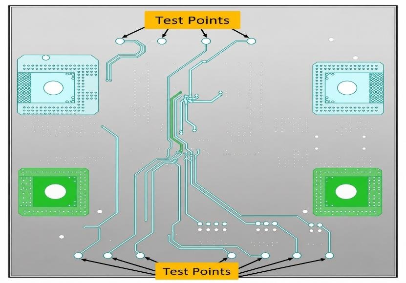
The layout was optimized by:
- Removing unnecessary test-point routing
- Improving ground continuity
- Adding ground vias
- Reducing parasitic structures
- Improving routing around sensitive signal paths
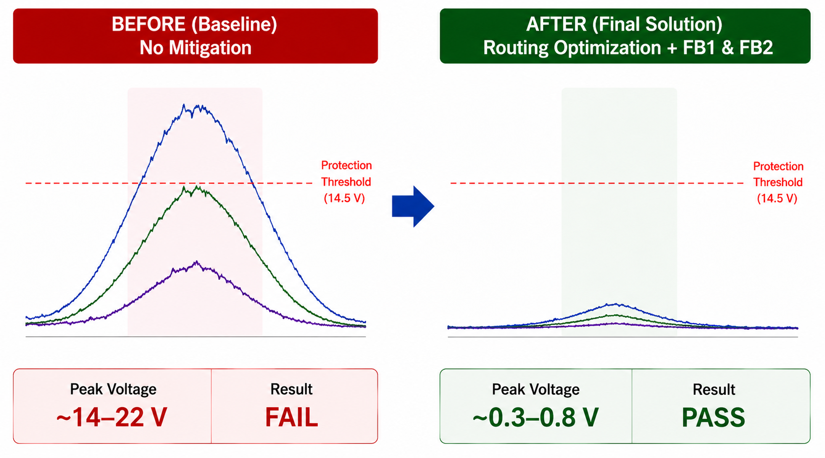
The impact was dramatic. Peak differential voltage dropped from approximately 14 V to 0.8 V. The majority of the susceptibility problem had been eliminated through layout optimization alone.
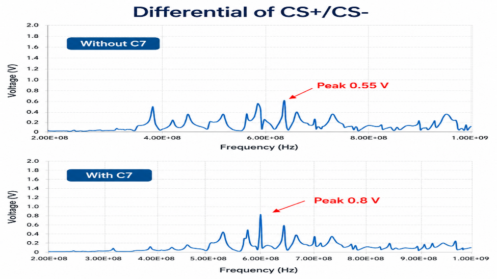
Attempt 3: Suppress Residual Noise
Although the layout improvements addressed the dominant coupling mechanism, some common-mode energy was still reaching the protection circuitry.
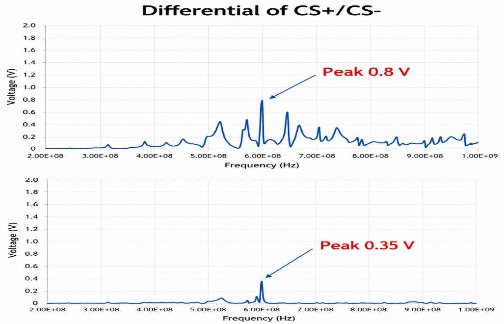
Ferrite beads were added to the CS+ and CS− signal paths and evaluated in simulation. The resulting voltage peaks fell even further.
Peak differential voltage dropped from approximately 0.8 V to 0.35 V.
From Failure to Pass
The optimized design was then validated through physical testing.
The simulation had accurately predicted the dominant failure bands. It had correctly identified the susceptible pins. It had correctly predicted the impact of each mitigation strategy.
Most importantly, the final hardware behaved exactly as expected.
The combined PCB and ferrite-bead optimization reduced peak coupled voltage from approximately 14 V to 0.35 V and enabled successful radiated immunity performance across the original failure bands.
Why This Matters
Radiated immunity failures are often discovered late in development, when every design change carries schedule and cost implications. The challenge is rarely identifying that a failure exists. The challenge is understanding why it exists and determining which change will actually fix it.
In this project, virtual analysis provided visibility that traditional testing could not. Instead of relying solely on repeated chamber tests and board iterations, the team could identify the dominant susceptibility path, evaluate multiple mitigation strategies, and focus hardware changes on the areas that mattered most.
The result was not just about passing EMC testing. It was a clear understanding of the failure mechanism and a faster path to resolution.