When a Sensor Passes Every Test Except One, Every Single Time!
At a Glance
The Problem With Trying the Right Things in the Wrong Place
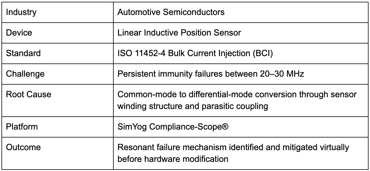
An automotive inductive position sensor was failing Bulk Current Injection (BCI) testing during customer-level validation. The failure was consistent: between 20 MHz and 30 MHz, the same frequency band, every time. The test itself was standardised and repeatable, with a common-mode current injected through a clamp positioned 150mm from the device, at Test Severity Level IV (200mA), across six cables covering power, ground, and signal lines. But the glitch kept happening.
The team then tried the obvious approach. Filtering was applied across power and signal paths. That’s the standard first response to any BCI immunity problem. But, the results barely helped and the failures stuck around..
This is the point where BCI debugging becomes genuinely difficult. The test injects a common-mode current into the cable harness. That current travels through cables, onto the PCB, through passive and active structures, and eventually reaches IC pins. Somewhere along that journey, energy converts from common-mode to differential mode, and if the differential voltage at a sensitive pin exceeds the IC's immunity threshold at a given frequency, the device fails.
The problem is that you cannot measure that journey directly in a lab. You can measure the injected current and observe that the device fails. What you cannot observe is the path the energy takes between those two points — which structures it travels through? Where does it convert from common to differential mode? Which components are amplifying it, and why is 20–30 MHz the vulnerable range rather than elsewhere?
Without that visibility, every filtering attempt is a hypothesis. And limited schematic design flexibility meant that repeated trial-and-error cycles were expensive and slow.
What Makes Inductive Position Sensors Particularly Challenging
Before describing what the simulation revealed, it helps to understand why inductive position sensors present a specific EMC challenge that doesn't apply to most ICs.
A conventional IC sits on a PCB and interacts with the electromagnetic environment through its power supply lines and signal traces. An inductive position sensor does something different: it generates its own alternating magnetic field through a winding structure and measures changes in that field caused by a nearby conductive target moving. The sensor IC, the winding, the PCB, and the target are all electromagnetically active participants in the measurement.
That winding structure has significant physical dimensions. And large coils have high parasitic capacitance, particularly between the sensor and nearby conductive surfaces, such as a test table. In a BCI test environment, that parasitic capacitance becomes a low-impedance path for common-mode noise. The sensor itself becomes a coupling mechanism.
This is why conventional filtering on signal and power lines didn't solve the problem. The dominant noise path wasn't through those lines. It was through the sensor structure itself.
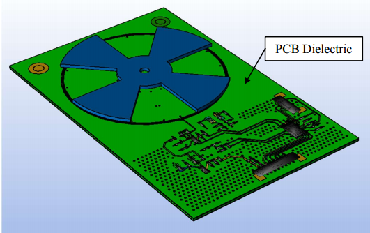
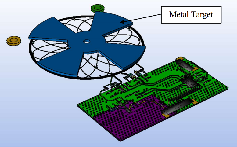
Positioning Sensor PCB with a Metal Target
Recreating the BCI Environment Virtually
To gain visibility into the actual coupling mechanism, the team recreated the complete ISO 11452-4 BCI test environment in SimYog's Compliance-Scope® platform.
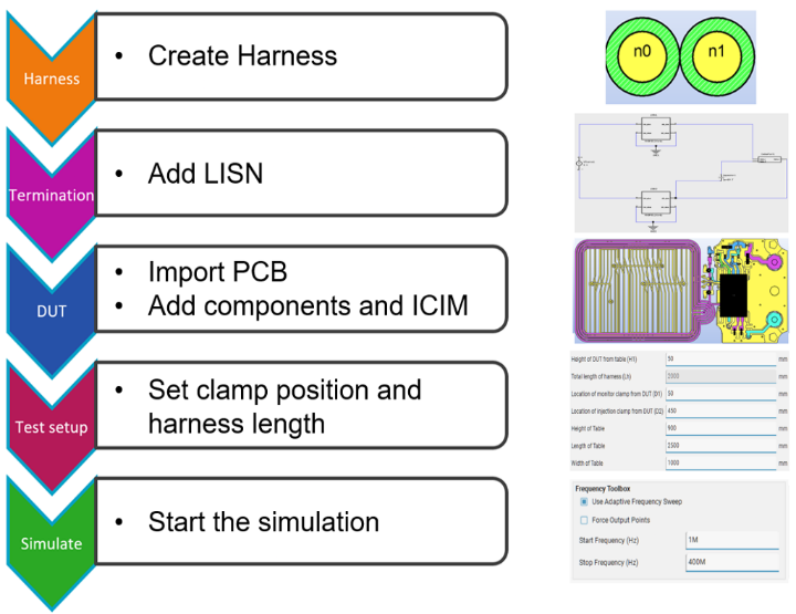
The virtual model included:
- The cable harness, modeled with full-wave electromagnetic accuracy
- The BCI injection clamp, represented as a calibrated network model
- The LISN and load configuration (standard test-bench components for BCI testing)
- The PCB, imported directly from the design files with all passive components and their parasitic parameters
- The sensor winding structure and the parasitic capacitance to the test table
- The IC, represented using an IC Immunity Model derived from DPI measurements, following the IEC 62132-4 standard.
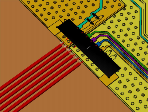
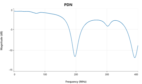
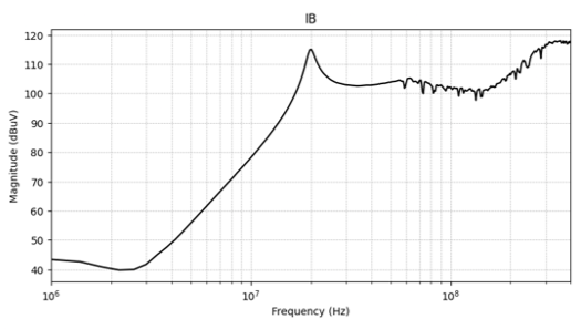
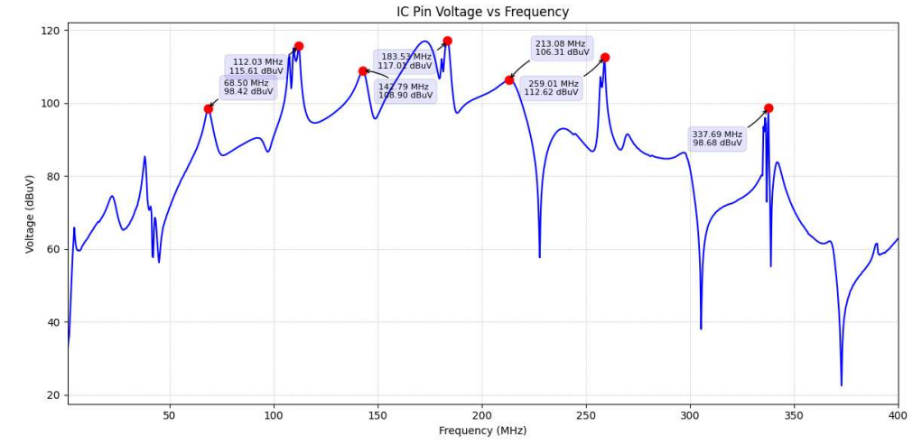
That last element deserves particular attention. Conventional EMC simulation treats ICs as passive impedance blocks. The ICIM approach goes further: it characterises each IC pin's immunity threshold (their impedance) as a function of frequency, based on actual DPI measurements of the device. This means the simulation doesn't just predict how much voltage appears at an IC pin. It can predict whether that voltage will cause a functional failure, at which frequencies, and by how much margin.
This is the difference between a simulation that tells you what's happening electrically and a simulation that tells you whether it matters.
What the Simulation Revealed
The simulation reproduced the BCI failure behaviour and quickly pointed to the cause.
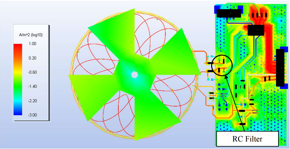
Common-mode noise from the injected clamp current travelled through the harness to the PCB, then into the sensor's primary winding. From there, it coupled into the secondary winding, which connects directly to the sensitive IC pins, and arrived as differential-mode voltage at the IC input.
Two things were amplifying this process.
First, the parasitic capacitance between the sensor winding and the test table was creating a dominant common-mode coupling path. Because the sensor has large physical dimensions, this capacitance is not a minor detail. It was channeling significant common-mode energy into the sensor structure at the frequencies where the device was failing.
Second, the RC filter network connected to the secondary coil was resonating at the failure frequencies. The combination of filter component values and PCB parasitic inductances was creating a resonance condition that amplified the differential voltage appearing at the IC pins, pushing it above the immunity threshold precisely in the 20–30 MHz band.
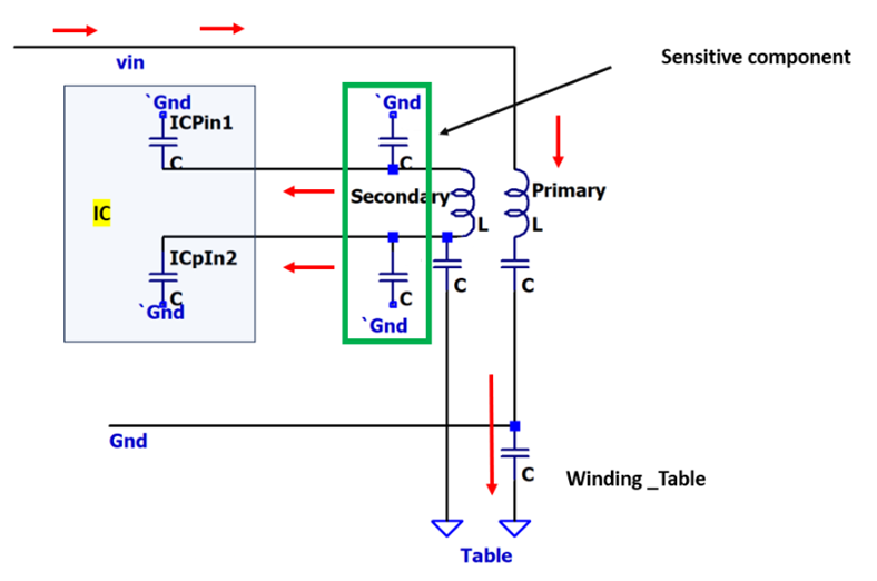
Current density analysis confirmed this. When the simulation was run at the resonant frequencies, and the resulting current distribution was visualised across the PCB, the RC filter connected to the secondary coil showed the highest current density. The filter network wasn't suppressing the noise. At resonance, it was amplifying it.
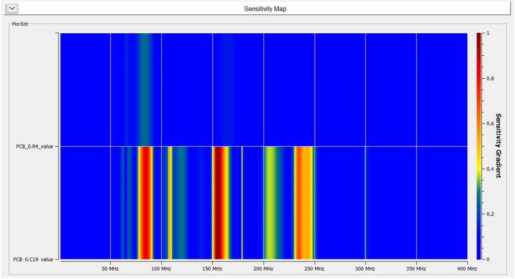
Sensitivity analysis provided the final layer of insight. By applying a ±10% perturbation to each filter component and observing the resulting change in IC pin voltage across the frequency range, the simulation ranked each component by its influence on the failure behaviour. Two components,a specific resistor and a capacitor in the secondary coil filter network, emerged as dominant across the critical frequency band. Small changes to those two components would have the largest effect on the immunity margin.
At this point,the team did not just know that the design was failing, but they knew exactly why, and exactly which components to change.
Evaluating Fixes and Experimenting
With the failure mechanism comprehended and the sensitive components identified, the next step was finding the right mitigation. Rather than modifying hardware and returning to the chamber, the team used Compliance-Scope® 's What-If analysis capability to evaluate multiple filter and snubber configurations virtually.
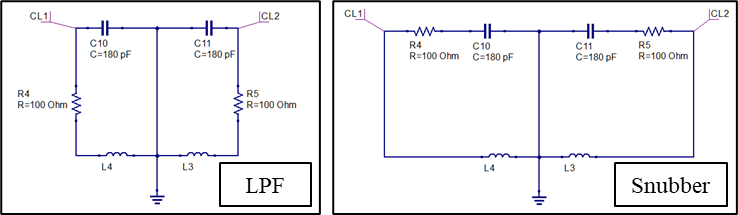
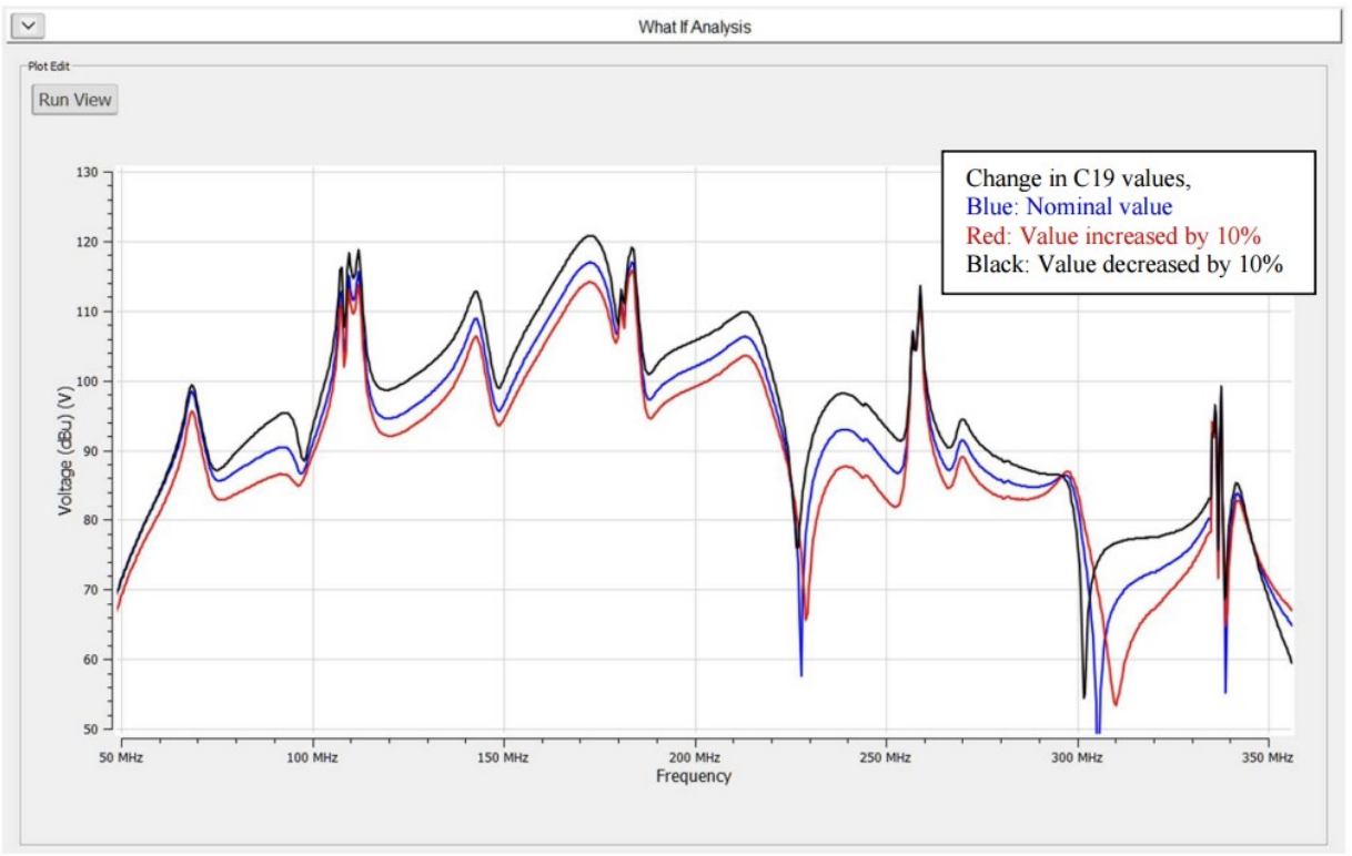
What-If analysis in this context means: take the identified sensitive components, replace them with alternative values in the simulation, and observe the resulting change in IC pin voltage — without re-running the full electromagnetic simulation from scratch. The What-If capability does this in a fraction of the time of a full re-solve, making it practical to evaluate dozens of configurations in the time it would take to fabricate one modified board.
The team evaluated multiple low-pass filter configurations and snubber options, built around the same components (180pF capacitors and 100Ω resistors, paired with the board's existing inductors). The results showed clearly how different resistor and capacitor combinations affected the resonant behaviour and the differential voltage at the IC pins across the failure region. Some configurations shifted the resonance frequency without suppressing the peak amplitude. Others reduced amplitude in one frequency region while making another worse — a pattern the team had already encountered in physical testing with earlier filtering attempts.
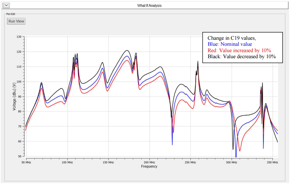
Eventually, the simulation identified an optimised low-pass filter configuration that reduced IC pin voltage below the immunity threshold across the critical 20–30 MHz band without degrading overall circuit performance.
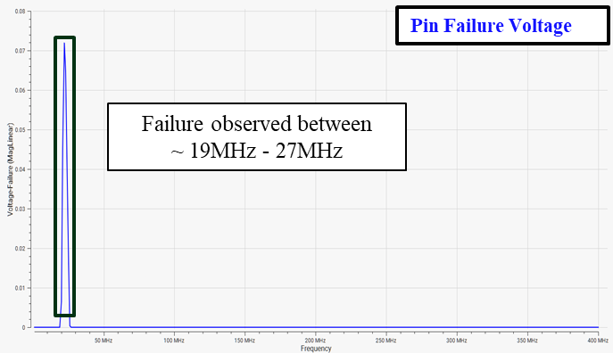
That configuration was then implemented in hardware and validated physically. Testing confirmed that the previously observed failure behaviour in the 20–30 MHz range had been successfully mitigated. The simulation had predicted failure between 19 and 27 MHz. The lab had measured failure between 20 and 30 MHz. The correlation was close enough to treat the virtual environment as a reliable guide for mitigation decisions.
What This Means in Practice
The conventional BCI debug cycle looks like this: test, observe failure, hypothesise a fix, modify the board, rebook the chamber, retest. Each iteration takes weeks. Each board modification introduces risk. Each chamber session has a cost. And if the root cause is misunderstood, those iterations can continue for a long time without resolution.
Here, that entire cycle happened in simulation instead. The filter configurations that wouldn’t have worked out were discarded before any hardware was modified. The filter configuration that did work was validated virtually before it was implemented. The hardware test became a confirmation, not an experiment.
For inductive position sensors like this one, the weight of testing is compounded by the complexity of the coupling mechanism. The failure in this case wasn't in the power supply filter, or the signal line terminations; the places a conventional debugging approach would focus first. It was in the resonant behaviour of a secondary winding filter network, driven by parasitic capacitance between the sensor and the test table. That mechanism is not intuitive. Without simulation, finding it requires a systematic process of elimination that takes considerably longer than recreating the environment virtually.